
Equipment
Dektak 6M
Price on request
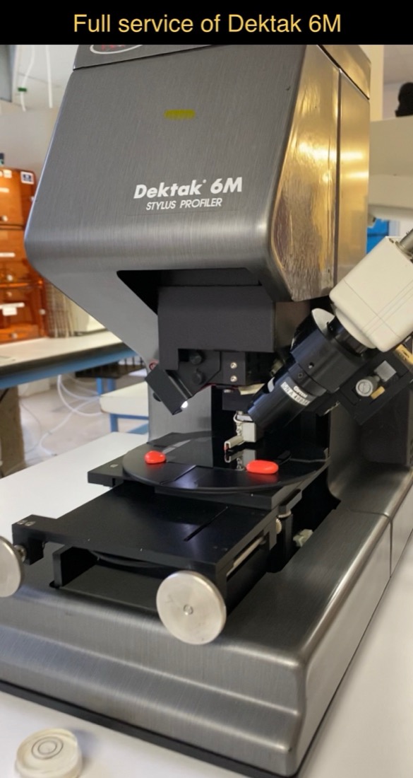
The Bruker/Veeco Dektak 6M is a contact stylus surface profiler for measuring step height, roughness, and waviness across a wide vertical range — a mainstay for thin-film and coating thickness verification.
The Bruker/Veeco Dektak 6M is a contact stylus surface profiler for measuring step height, roughness, and waviness across a wide vertical range — a mainstay for thin-film and coating thickness verification.
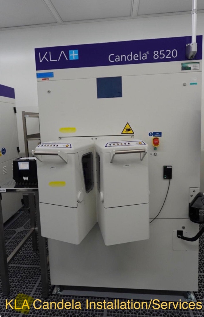
The KLA Candela 8520 is a dual-port optical surface inspection system built for high-volume wafer and substrate scanning, detecting micro-defects, particles, and surface anomalies at production throughput.
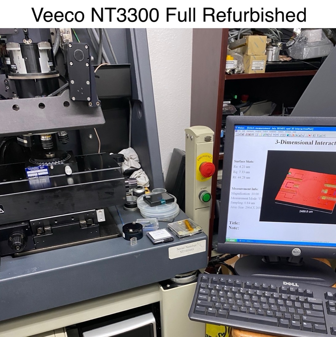
The Veeco NT3300 is a non-contact 3D optical profiler using white-light interferometry to measure surface roughness, step height, and film thickness with sub-nanometer vertical resolution. A compact, production-friendly footprint makes it a popular choice for semiconductor, MEMS, and data-storage surface metrology.
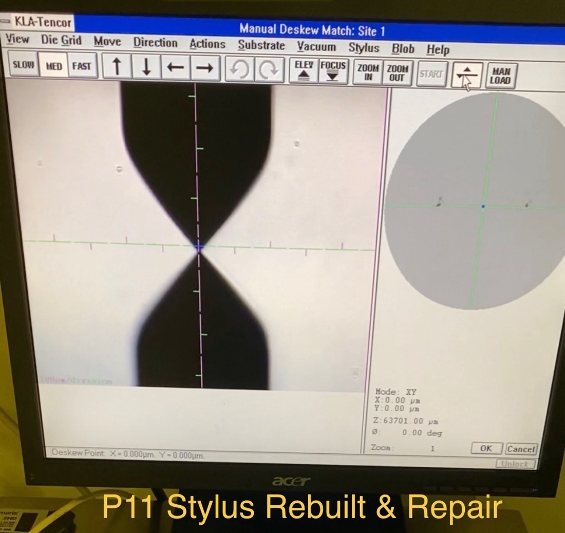
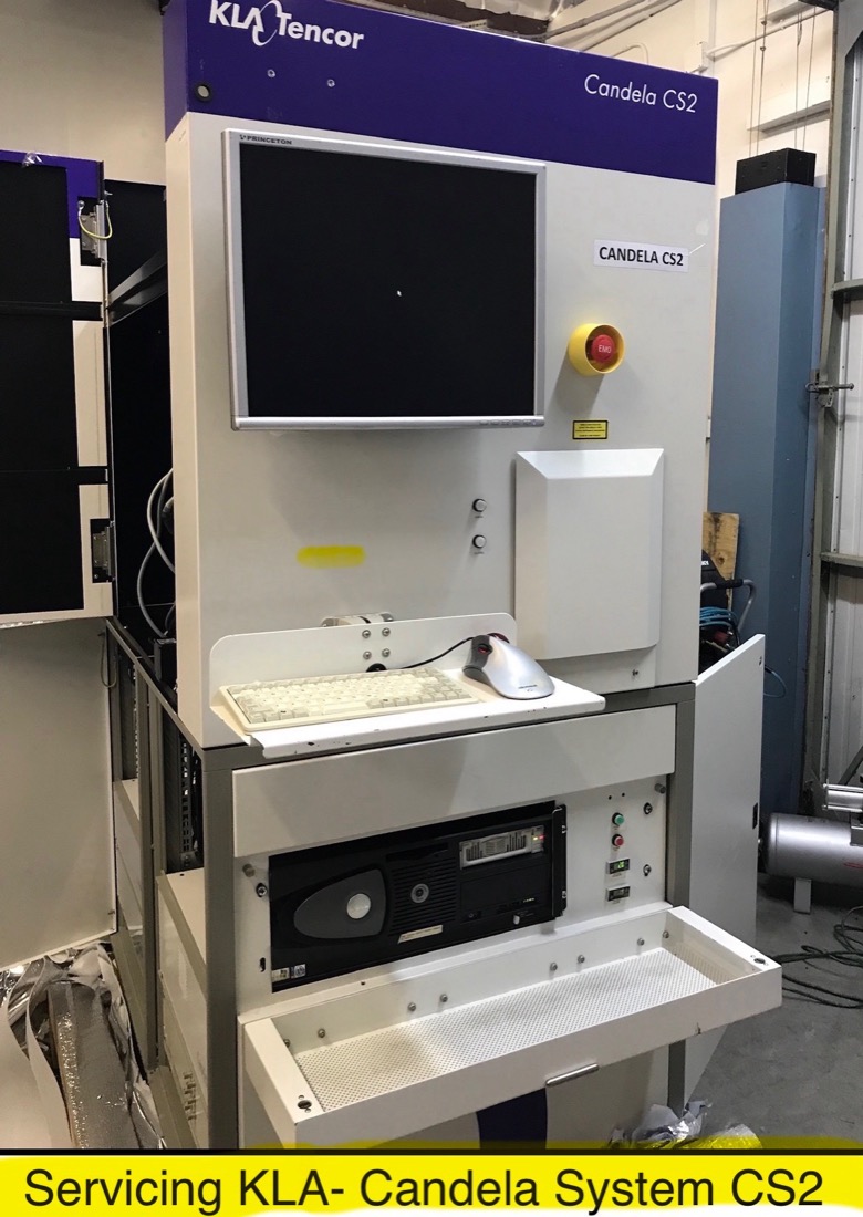
The KLA-Tencor Candela CS2 is a high-throughput optical surface analyzer for detecting and classifying defects, scratches, and particles on semiconductor wafers and disk media. Multiple optical channels capture surface topography and reflectivity data in a single non-contact scan, well suited to high-volume production monitoring.
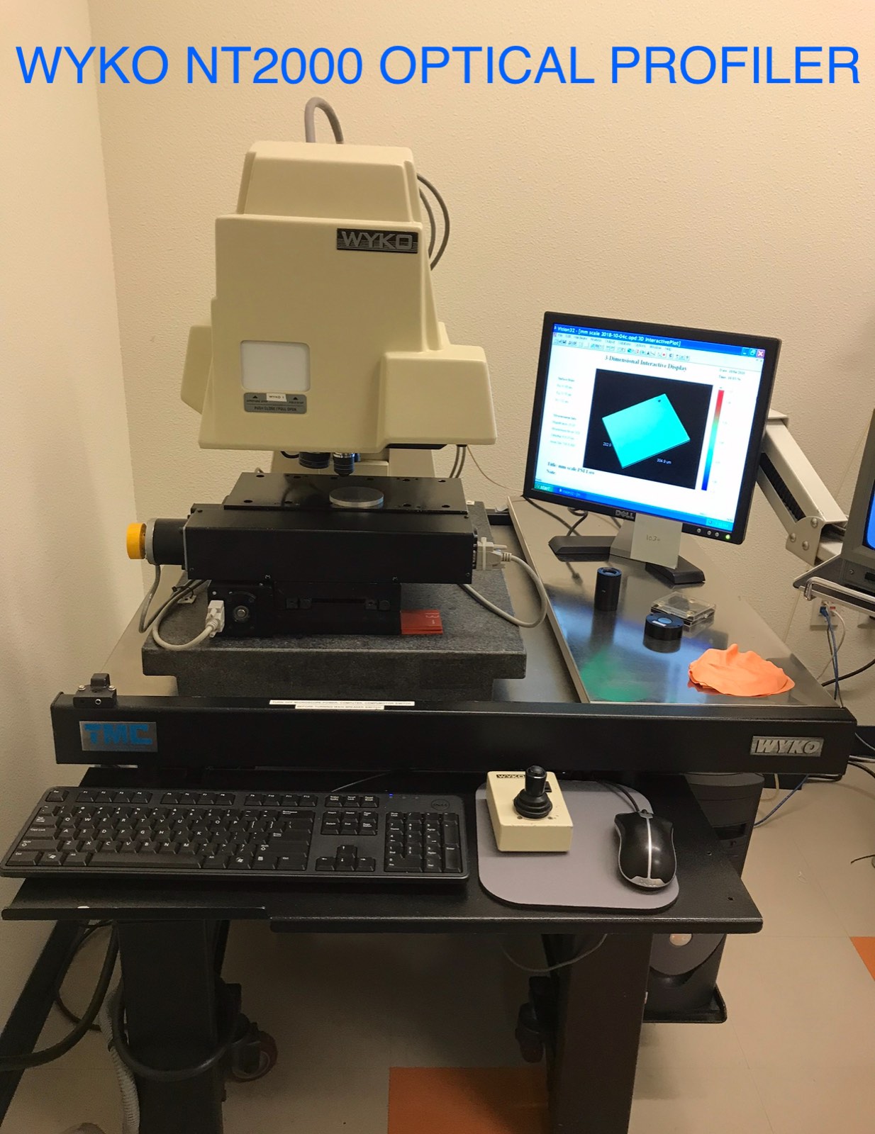
An automated optical surface profiler designed for semiconductor manufacturing, using non-contact interferometry for 3D surface topography measurement.
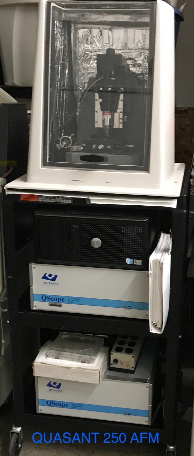
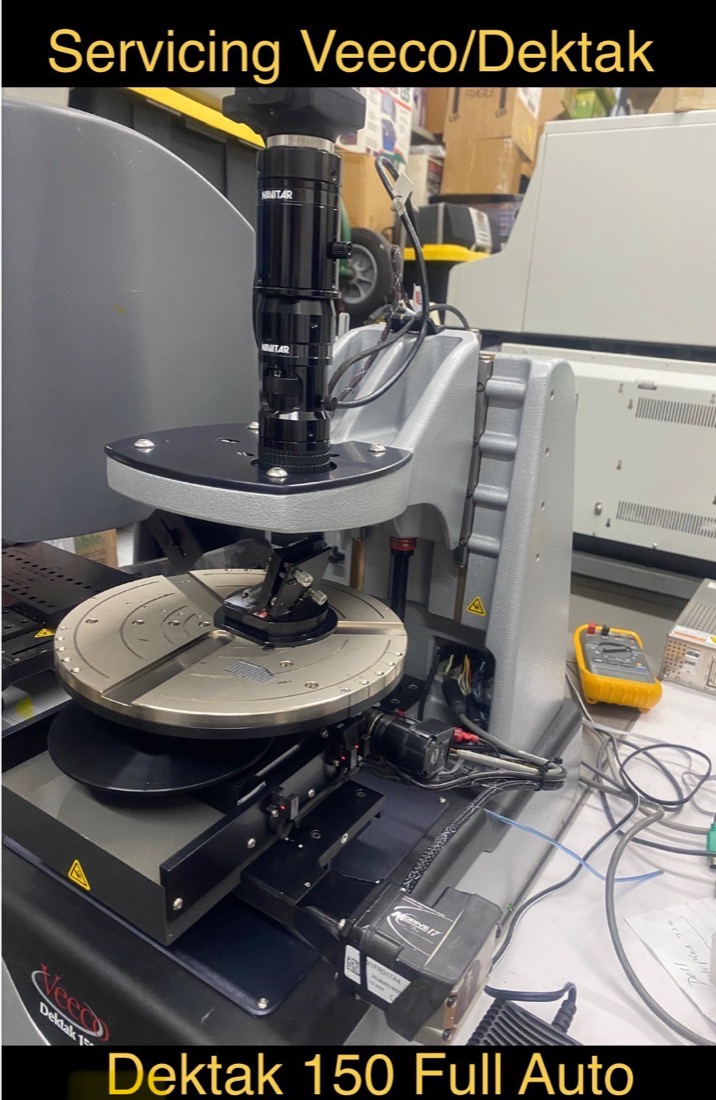
A surface imaging system with a 6″ × 6″ maximum sample stage, a 65mm maximum sample height, and a motorized Z-translation stage. Features an integrated 200X video microscope for sample viewing.
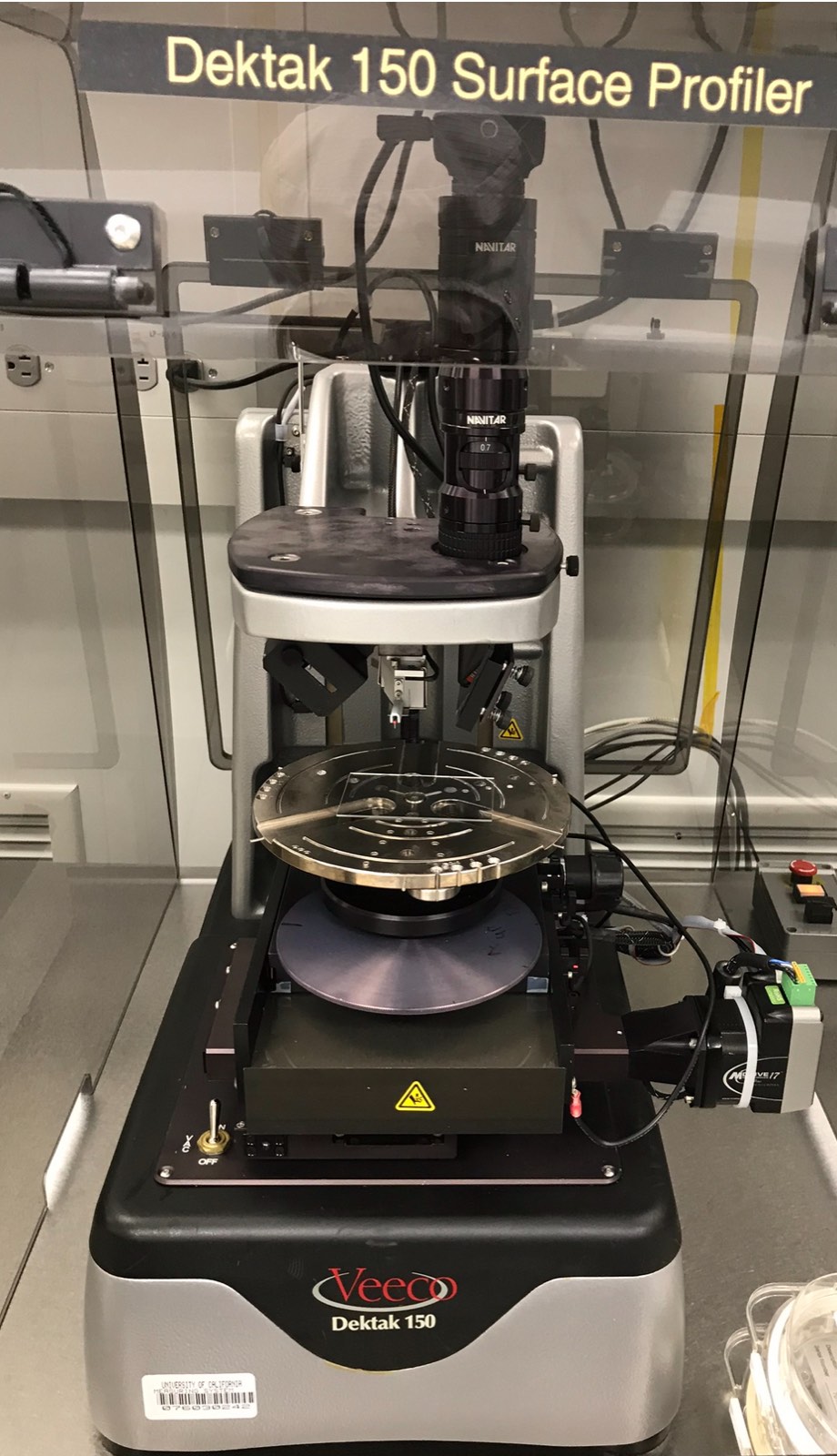
A surface profiler with a 150mm (6-inch) maximum sample size, a 55mm scan length, and a vertical resolution down to 1 Ångström at its best. Uses a contact stylus to measure surface roughness and step heights, with a vertical range of up to 524µm. Available in a Full Auto configuration with motorized sample loading and automated measurement recipes for higher-throughput environments.
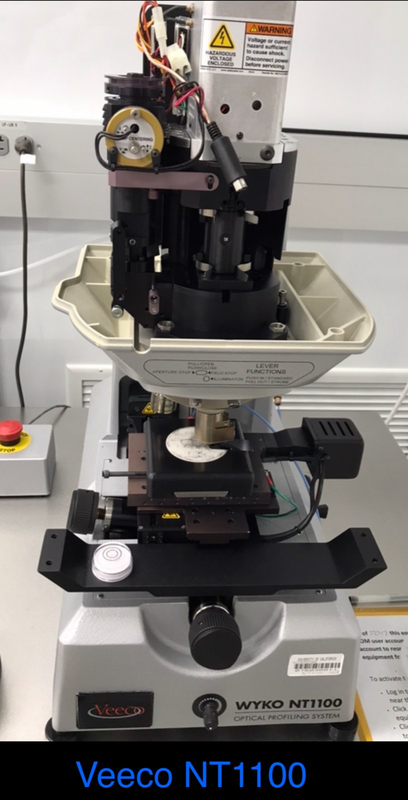
A non-contact 3D surface metrology system using white light interferometry to measure surfaces from sub-nanometer roughness to millimeter-high steps. Offers two measurement modes — VSI and PSI — with different resolutions and ranges, and a variety of objectives for different magnifications.
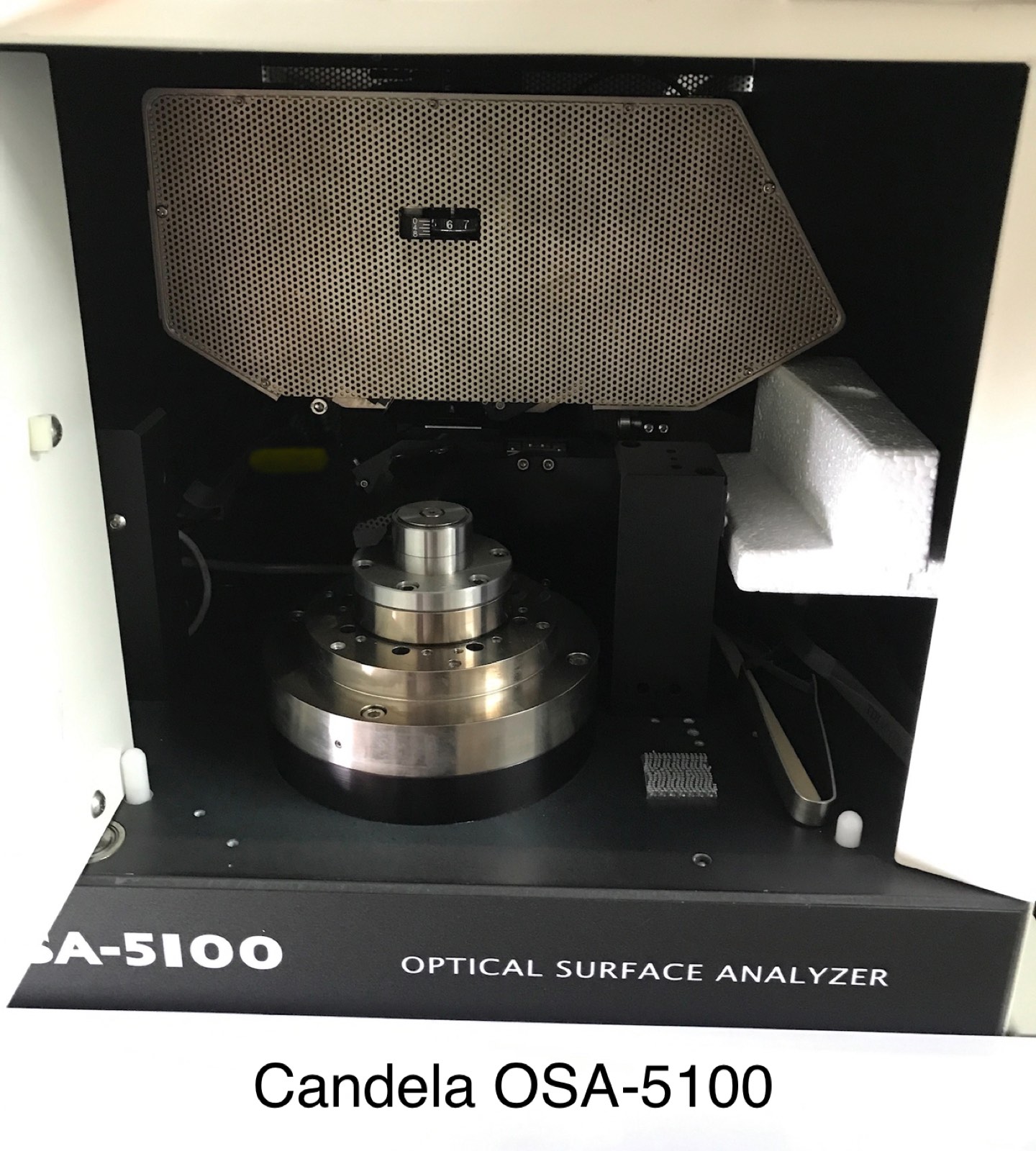
The KLA Candela Optical Surface Analyzer (OSA) 5100 is a semiconductor and photovoltaic wafer metrology system that analyzes surface properties like thickness, uniformity, and texture using advanced optical techniques.
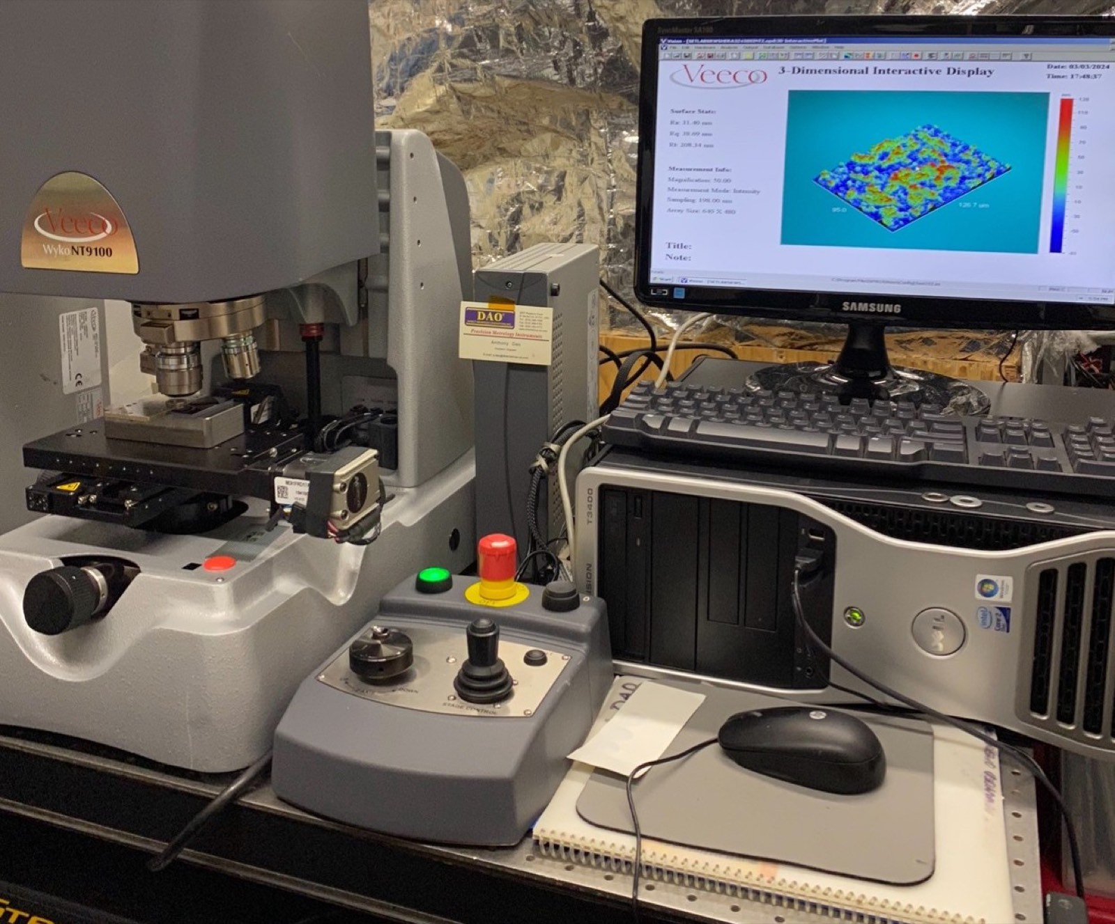
Accurate surface topography with sub-nanometer vertical resolution across all magnifications. Motorized, programmable stage with stitching for large-area measurements. Non-contact 3D surface metrology with dual-LED illumination and full 2D/3D data analysis & visualization. Objectives: standard 5X, 10X, 20X, 50X on a motorized turret — magnification from 0.75X to 100X. Field of view: 0.55x, 0.75x, 1x, 1.5x, 2x. Automated 100mm Z-axis with ±6° tip/tilt stage and 100mm XY travel.